
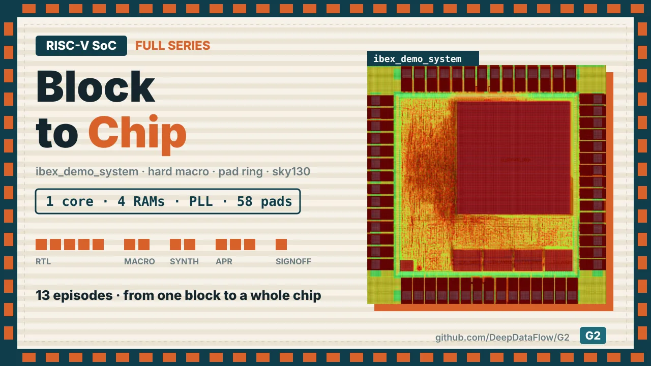
A block is not a chip. In our previous series, RISC-V RTL-to-Signoff, we took one RISC-V core, lowRISC's Ibex, from RTL to signoff as a single block. In this series we build a chip around that core. It gets memory and peripherals, a PLL, real IO pads, and the core itself goes in as a hard macro. Then we synthesize, place, route and sign off the whole chip in G2.
This article is the written companion to the 13 videos. Each section has the episode, the decisions behind it and the numbers it produced. Every file is in the G2_demo_sky130 project.
| Design | lowRISC Ibex Demo System: bus, RAM, GPIO, UART, SPI, PWM, timer, JTAG debug |
| Process | SkyWater 130 nm (sky130 HD standard cells) |
| Tools | Yosys, OpenROAD, OpenRCX, OpenSTA, all inside G2 |
| Chip | 1.8 × 1.8 mm die, 58 pads, 6 macros (core, 4 RAMs, PLL), 115,854 instances after fill |
| Result | Hold met; setup −1.445 ns at the slow corner, so 24.1 MHz instead of the 25 MHz target |
Part 1: The pieces of a chip
#1From block to SoC
 2:02
Watch on YouTube ↗Watch on Bilibili ↗
The SoC is lowRISC's Ibex Demo System: a bus, a RAM, GPIO, UART, SPI, PWM, a timer and a JTAG debug module around one Ibex core. It was written for an FPGA. Two of its parts will change: u_top is the core, and u_ram is 128 KiB of dual-port memory.
In G2, the SoC becomes a new block, ibex_demo_system. The name uses underscores because G2 uses the block name as the top module for synthesis and place and route, and Verilog names can't contain dashes. One click creates the spec page and the block's folders in implementation, scripts and the design data manager (DDM). The hierarchy puts the SoC at level 0 and the core from series 1 at level 1 inside it.
The first spec field is speed: 25 MHz. The core signed off at 25.56 MHz at the slow corner, and the SoC can't run faster than its core. The standard-cell field opens the block's stdcell.cfg, and that file is what the flows read. This matters again in synthesis.
#2A dual-port RAM macro
 2:25
Watch on YouTube ↗Watch on Bilibili ↗
The SoC's RAM is 128 KiB and dual-port: one port for data and one for instruction fetch. On an FPGA that is block RAM. On a chip it is a memory macro, and our library only has the single-port RAMs from the core's instruction cache.
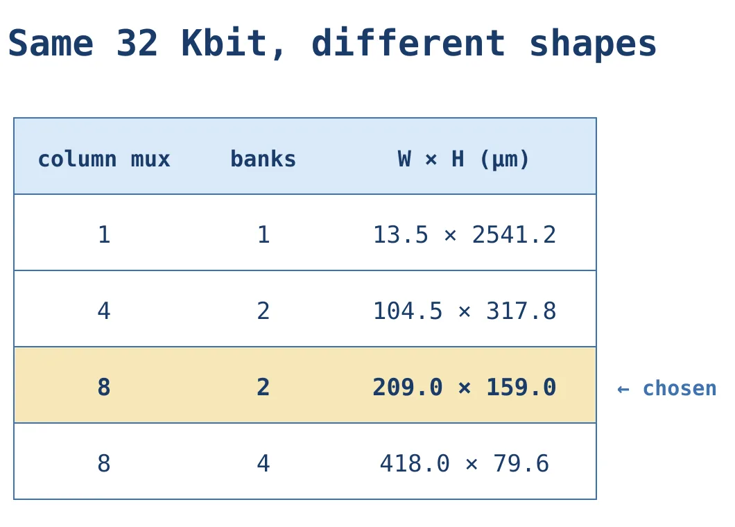
We made two decisions. First, 16 KiB is plenty for the demo software, and 128 KiB would be huge in sky130. Second, the generator's dual-port RAM has no byte write mask, so the 32-bit memory is built from four 8-bit macros, one per byte lane.
FakeRAM2.0 makes timing and layout views for a memory that doesn't really exist, which is ideal for flow work. The same 32 Kbit can take very different shapes:
Always read the generated model. This one registers the address and then reads the array, so data comes out two cycles late. The liberty and our RAM wrapper both say one cycle, so we replace the model with a one-cycle version. The liberty comes out as a single typical corner. The project has four corners, so we write four copies with the right voltage and temperature in the header; the timing is the same in each, as with the series-1 RAMs.
In G2's library manager (LIM) the order of operations matters: Find, Build all, then Fill. Fill matches each liberty to a corner using the built pages, so if it runs first nothing matches. The result is two ports with 12 address bits and 8 data bits each, and 0.218 ns from clock to data.
#3Fit the SoC around a hard core
 2:07
Watch on YouTube ↗Watch on Bilibili ↗
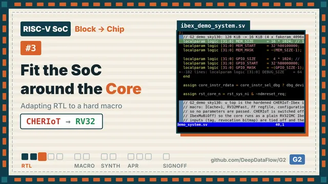
The SoC's RTL goes into DDM as rtl v01, copied from the demo repository, which stays untouched. Then comes the catch: the core we hardened in series 1 is the CHERIoT version of Ibex. Its ports don't match this SoC. It has CHERIoT and lockstep ports the SoC has never heard of, and the SoC passes parameters a finished macro can't take.
We keep the macro and adapt the SoC:
- CHERIoT is switched off, so the core runs as a plain 32-bit RISC-V.
- The extra inputs are tied off and the extra outputs left open.
- The parameters are removed, so the SoC gets exactly the configuration we hardened.
- The RAM shrinks to 16 KiB, and every edit is tagged so it can be found later.
A RAM wrapper maps the 32-bit memory onto the four byte-wide macros, with each byte's write enable as its mask bit. Before any synthesis, a quick elaboration check runs with the core and RAMs as black boxes. Without one extra flag, slang stops: the debug module uses a signal before declaring it. Simulators let that slide; slang doesn't. With the flag the design links: one core and four RAMs, with port names and widths that match the real macro.
#4Real-chip clocking
 2:19
Watch on YouTube ↗Watch on Bilibili ↗
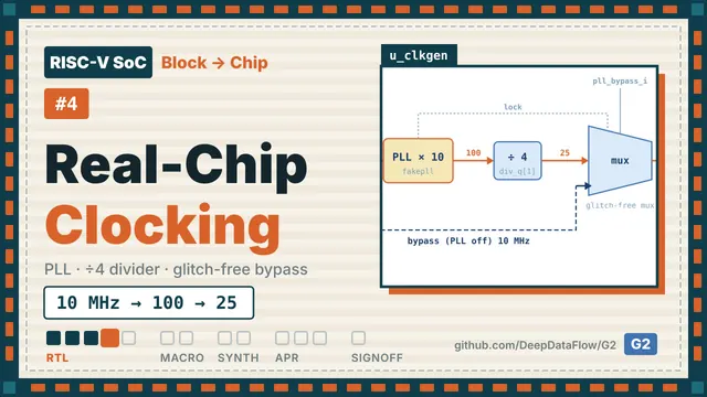
On the FPGA board the clock came in on a pin. A real chip makes its own: a 10 MHz reference, a PLL that multiplies it by ten, a divider down to 25 MHz for the core, and a bypass so the chip still runs if the PLL doesn't.
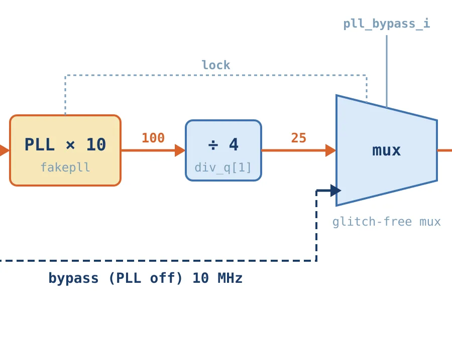
sky130 has no PLL we can use, so we make a fake one, like the fake RAMs: realistic layout and timing views with no circuit inside. One choice is deliberate: there is no timing arc from the reference to the output. A PLL's output is a new clock, and the constraints will say so.
The clock generator, clkgen, is the careful part of rtl v02. A two-bit counter divides the PLL clock, and its top bit is the 25 MHz clock. Each clock has its own clock gate, each gate's enable is synchronized in its own clock domain, and an enable only turns on after the other one is off. Out of reset the reference runs while the PLL locks. A reset synchronizer releases reset cleanly.
The slower clock also breaks the SPI host: 25 MHz over a 12.5 MHz SPI clock leaves a toggle count of one and a zero-bit counter. We keep the original ratio, a quarter of the system clock. Three caveats remain: in bypass the UART baud rate is wrong, the bypass pin may only change in reset, and the PLL is a stand-in.
#5Real pads
 2:40
Watch on YouTube ↗Watch on Bilibili ↗
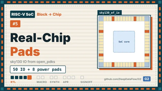
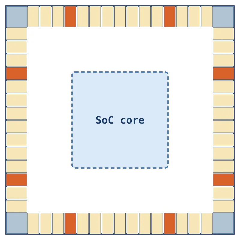
A chip talks to the board through pads. sky130's IO library in skywater-pdk has layout and Verilog but no timing, and we can't synthesize or sign off without timing. open_pdks builds the full set, including Efabless's wrapped pads that every Caravel chip uses, with timing for every corner. LibreLane's pad configuration tells us which cells a proven sky130 pad ring uses: a general-purpose IO pad, core and IO power pads with ESD clamps, a corner cell and filler slices.
A small installer copies five cells, each with a liberty for our four corners, into G2's PDK. In LIM each cell gets its own entry, because an entry holds one liberty per corner. All 20 liberty files match. (Two small LIM bugs turned up here: Fill skips symlinks, and a page title is wrong.)
The chip top in rtl v03 keeps the SoC's port names, now as bond pads: 50 signal pads and 8 power pads. The pad wrappers take their high-voltage enables from the pad's own tie-high and tie-low outputs, as Caravel does. While we were here, we shrank three 128-byte FIFOs built from flip-flops, which were almost two thirds of every flip-flop in the chip, to 16 entries each.
Part 2: Turning the core into a hard macro
#6Make the block macro-ready
 2:51
Watch on YouTube ↗Watch on Bilibili ↗
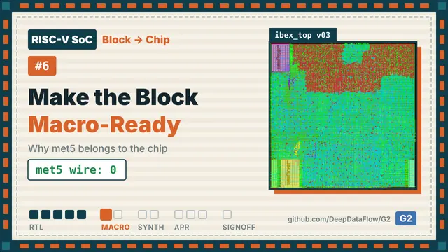
This is the rule for hard blocks: the parent owns the top metal. A macro's abstract view blocks every metal layer the block uses. Our series-1 core used metal 5 for its power grid and routing, so the whole macro was closed on metal 5. The chip's metal-5 power straps stopped at its edge, and in our practice run the chip-level power check reported the core's supply pin as unconnected. The core would have had no power.
The fix is a convention: a block stops at metal 4, and the chip drops vias from metal 5 straight onto the block's metal-4 power pins. We re-ran the core as build v03, leaving series 1's build untouched, with three script changes:
- Routing stops at metal 4, for signals and clocks.
- Every stage reads those settings, not only the floorplan.
- The power grid loses its metal-5 straps. The floorplan script now also looks for a design's own power script and a pad ring script, which the chip will use.
Routing took 14 minutes and ended with 120 violations, a few fewer than before, and the line we wanted: 0 µm of wire on metal 5. After post-route and finish there were 130 violations, the price of one less layer and fine for a demo.
#7Block to hard macro
 2:48
Watch on YouTube ↗Watch on Bilibili ↗
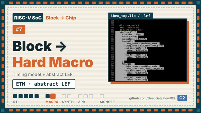
A parent design needs three views of a hard block: parasitics, a timing model per corner and an abstract layout.
- Parasitics: OpenRCX extracts the new layout in four corners in under a minute.
- Timing model: OpenSTA's
write_timing_modelwrites the core as one cell, with setup and hold checks on its inputs, clock-to-output delays that include its own clock tree, and the clock-tree latency itself. The stock script gave every corner's model the same name, so corners collided. We name each one after its corner. Note that the model's area is the cell area, not the macro's footprint. - Abstract LEF: tie nets that the router treated as power go back to signals, or they would show up as empty power pins. The abstract blocks every layer the block uses, and the power pins keep only metal 4. The raw abstract lists thousands of internal power shapes without the vias that join them, and one level up they look floating.
The result is an 850 × 850 µm macro with 930 pins, power on metal 4 and nothing at all on metal 5. The views agree: 928 signal bits in the LEF, the netlist and the timing model. The core goes into LIM as hard IP. Two corners match, the two we signed off; the other two have no timing model and aren't used.
Part 3: Constraints and synthesis
#8Constrain a real chip
 2:14
Watch on YouTube ↗Watch on Bilibili ↗
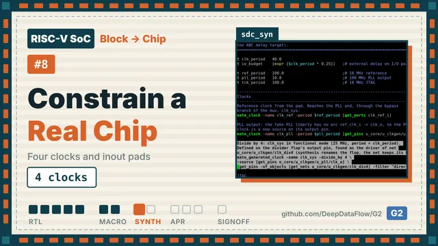
The synthesis constraints, sdc_syn v01, are driven by one number: the system clock at 40 ns. There are four clocks. The reference is on its pin. The PLL output is a new clock defined on the PLL's output pin, which is why the fake PLL has no timing arc. The system clock is generated from it, divided by four:
create_clock -name clk_ref -period $ref_period [get_ports clk_ref_i]
create_clock -name clk_pll -period $pll_period [get_pins u_core/u_clkgen/u_pll/clk_o]
create_generated_clock -name clk_sys -divide_by 4 \
  -source [get_pins u_core/u_clkgen/u_pll/clk_o] \
  [get_pins -of_objects [get_nets u_core/u_clkgen/clk_div4] -filter "direction == output"]
create_clock -name clk_tck -period $tck_period [get_ports tck_i]
Synthesis renames flops, so a flop name copied from the RTL won't exist in the netlist. Nets keep their names, so we ask for the pin that drives the divided-clock net. JTAG is its own clock, and the three groups are asynchronous to each other because the mux control crosses through synchronizers.
In functional mode the PLL is on, and case analysis on the bypass pin isn't enough. The bypass clock gate's enable comes from a flop, not a constant, so the reference clock still leaks onto every system flop: 4,599 pins with two clocks. Disabling the bypass gate's clock arc leaves each flop with one clock:
set_case_analysis 0 [get_ports pll_bypass_i]
set_disable_timing -from CLK -to GCLK [get_cells u_core/u_clkgen/u_icg_ref/icg]
Every port is now a bond pad, an inout, so timing sees each pad as an input and an output. The direction a pad doesn't use gets a zero delay and is excluded, so nothing is left unconstrained by accident. Output pads drive a 5 pF board load.
#9Synthesize the chip
 2:18
Watch on YouTube ↗Watch on Bilibili ↗
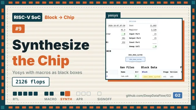
The chip gets a new implementation build: rtl v03 with the constraints from episode 8. G2 collects the libraries from the spec, 9 per corner: standard cells, the RAM, the core's timing model, the PLL and five pad cells. They come from the spec's library files, the ones the editors write, which is why we used the editors. The stock Yosys script counts flops by the wrong name for sky130; series 1 already fixed that, so we reuse its scripts, including the timing-driven one.
The run takes about 40 seconds: no errors, nothing unmapped, 11,692 instances and 2,126 flops, with every macro and pad in the netlist as a black box. Then the constraints meet the netlist. There are 22 endpoints without constraints, and every one is expected: the unused side of input pads, and the power pads. Each clock reaches the flops it should.
Pre-layout timing needs an honest reading. Setup on the system clock is −10.4 ns and reset recovery −21.4 ns, because the reset synchronizer drives 1,316 flops through no buffer at all, with 40.9 ns of slew. Synthesis doesn't buffer that net; placement will. With that one net taken out, every clock meets timing.
Part 4: Place and route the chip
#10Pad ring and chip power
 2:35
Watch on YouTube ↗Watch on Bilibili ↗
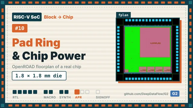
Place-and-route constraints are the synthesis ones with one change: board signals drive the input pads with a transition instead of a standard cell, because no standard cell can drive a pad. The die is 1.8 mm square with a 1.3 mm core. Fifty-eight pads need at least 1.6 mm per side, so the pads set the size, not the logic.
The pad ring script places IO sites around the die, then each side's pads in order, evenly spaced, with corners, filler slices, abutment and a bond-pad terminal for every port. One order matters: name the pad supplies before abutment. Otherwise abutment invents its own ring nets, the power pads never join the core supply, and nothing later fixes it.
# pad supplies first (add_global_connection ...), then:
global_connect
connect_by_abutment
place_io_terminals {*/PAD */VCCD_PAD */VSSD_PAD */VDDIO_PAD */VSSIO_PAD}
The power grid adds the pad supplies, a core ring tied to the power pads, and stripes that extend to the ring. Without -extend_to_core_ring the stripes stop short of the ring and the whole core grid floats. We found both of these the hard way in practice.
add_pdn_stripe -grid {grid} -layer {met5} -width {1.600} -pitch {27.200} -offset {13.600} -extend_to_core_ring
add_pdn_ring -grid {grid} -layers {met4 met5} -widths {10.0 10.0} -spacings {2.0 2.0} \
  -core_offsets {10.0 10.0} -connect_to_pads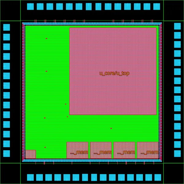
This is the payoff from episode 6: 32 metal-5 power straps run over the core, with 900 vias down onto its metal-4 power pins.
#11Place, CTS and post-CTS
 2:05
Watch on YouTube ↗Watch on Bilibili ↗
After placement the power check passes: every shape on the supply is connected. In practice it failed until the grid reached the ring and the core kept metal 5 free, which is why those fixes came first.
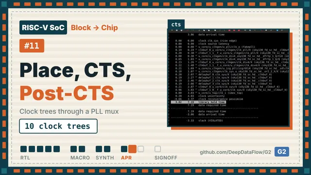
Clock tree synthesis builds ten clock trees. The system clock comes out of the glitch-free mux and reaches nine macro clock pins and 1,892 flops; JTAG gets its own tree.
Then the hierarchical part. The core's timing model says its own clock tree adds over five nanoseconds inside the macro: 3.8 ns to its pin plus 5.6 ns inside. The core's flops see the clock much later than the RAMs do, and that shows up as hold violations of −3.3 ns at the core's inputs. Post-CTS repair inserts 317 hold buffers and fixes every hold violation, including the core's.
One setup violation is left, at the clock divider. The divider's own output is now a clock-tree net, and it feeds back into its counter through that tree at 100 MHz. A real design would feed back from a separate flop; we note it and move on.
#12Route and finish
 0:55
Watch on YouTube ↗Watch on Bilibili ↗
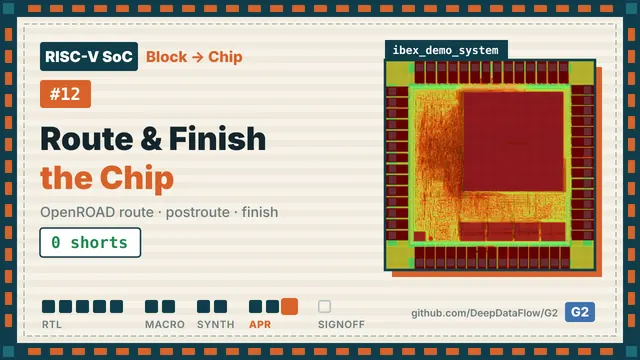
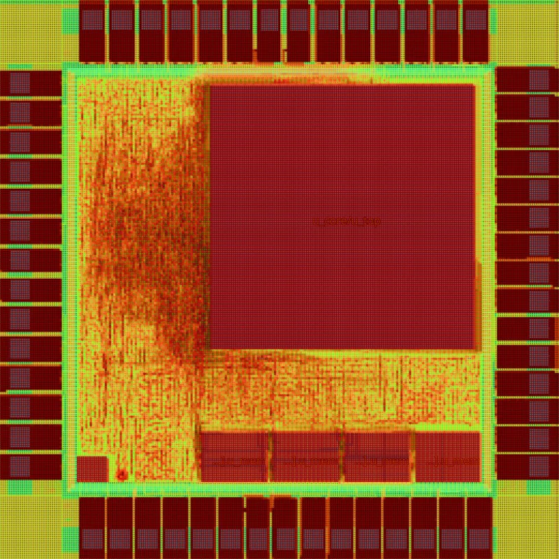
Routing the whole chip takes about ten minutes and ends with one violation, 1.07 m of wire and 106,115 vias. The core alone had 120: the chip core has room, and metal 5 over the macro is open to the chip. Post-route clean-up and finish, which adds fillers and writes the final netlist and layout, leave 2 violations and no shorts. The timing printed at finish still uses an ideal clock; the real numbers come at signoff.
Part 5: Signoff
#13Chip signoff
 2:56
Watch on YouTube ↗Watch on Bilibili ↗
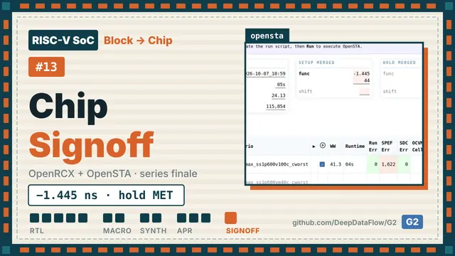
Signoff starts with real wires: OpenRCX extracts four corners in 18 seconds. The signoff constraints use propagated clocks, so the real clock trees count, and a smaller uncertainty, since skew is no longer guessed.
One section is needed only by a chip with real pads. The pad's timing depends on its drive mode. Our RTL ties those pins, but through nets with no driver, so timing can't see the values and assumes the slowest mode. Without the pad modes, an output pad takes 120 ns and the chip misses by 102 ns. With them it takes 6.9 ns, with 12.2 ns to spare.
OpenSTA then runs on the whole chip, with the core as its timing model and every pad, RAM and the PLL from LIM. The merged result:
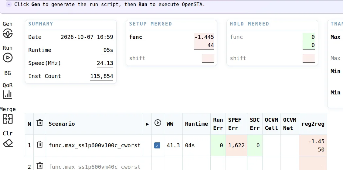
The worst path is the lesson of the series. The clock reaches the core at 7.8 ns. The core's timing model says its data address comes out 27.9 ns later: its own clock tree plus its logic. That leaves the SoC about 12 ns for the bus and the debug memory, and it needs 13.5. When you build with blocks, each block's output timing is a budget the chip has to live with. The chip runs at about 24.1 MHz instead of 25.
What we built, and what's left
From a core in series 1 to a chip: a dual-port RAM, a PLL with a safe bypass, 58 real pads, the core as a hard macro that leaves room for the chip, synthesis, place and route, and signoff. Everything ran in G2, and every hand-off went through the design data manager and the library manager.
What's left, and where to start:
- Setup −1.45 ns at the core's boundary. This is the core's clock-to-output budget; the next step is a faster core or a registered bus boundary.
- Output pad slew. The pad's transition tables are not mode-conditional, so this is a library modelling limit.
- An undersized clock gate on the PLL branch (max capacitance).
- The divider's feedback in the 100 MHz domain.
- Two DRC violations, and no DRC, LVS or GDS signoff in this series.
Watch and try it
- Videos: the YouTube playlist (English) and the Bilibili collection (Chinese).
- The core this series starts from: RISC-V RTL-to-Signoff.
- Next series: RISC-V Flip-Chip: Pads to Bumps removes the pad ring and compares this wirebond chip with a flip-chip version.
- The project: G2_demo_sky130. G2 itself is free as the Community Edition.
- Questions about G2 or running your own flows: support@deepdataflow.com. For licensing and partnerships: sales@deepdataflow.com.