
Same RTL, same constraints, two synthesis scripts: one misses timing by 16 ns, the other meets it. That is where this series starts. We take one real RISC-V core, lowRISC's Ibex with its instruction cache on, from RTL to signoff on SkyWater 130 nm, using only open-source tools inside G2: Yosys for synthesis, OpenROAD for place and route, OpenRCX for extraction and OpenSTA for signoff.
This article is the written companion to the 12 videos. Each section has the episode, the decisions behind it and the numbers it produced. Everything comes from the G2_demo_sky130 project on GitHub: clone it into your workspace, run make setup, and the project appears.
| Design | ibex_top: lowRISC Ibex with the instruction cache on, so 4 SRAM macros |
| Process | SkyWater 130 nm (sky130 HD standard cells) |
| Tools | Yosys, OpenROAD, OpenRCX, OpenSTA, all inside G2 |
| Block | 850 × 850 µm, about 2,400 flops, 98,222 instances after fill (70,818 fillers) |
| Result | Hold met (+0.17 ns); setup met except register-to-output, −1.74 ns on 8 address bits; 107 DRC |
Part 1: Synthesis
#1Yosys synthesis: from RTL to a first netlist
 4:01
Watch on YouTube ↗Watch on Bilibili ↗
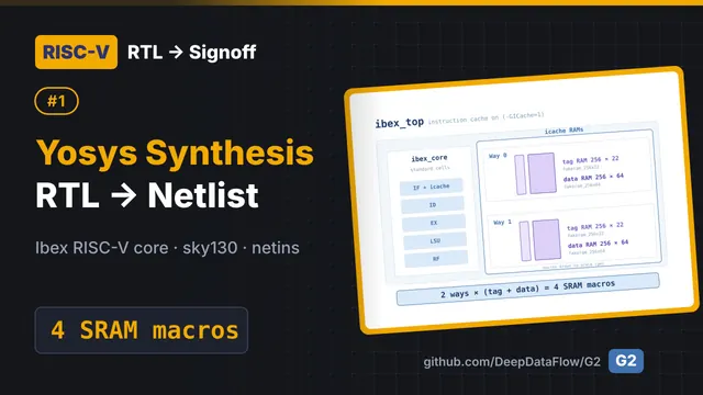
Our block is ibex_top, lowRISC's Ibex RISC-V core. Its spec binds the sky130 standard cells and two memory macros. With the instruction cache on, Ibex has two ways, each with a tag RAM and a data RAM: four SRAM macros, much closer to a real chip than a design with only standard cells. The memories live in G2's library manager (LIM) like any library, with a LEF and four timing corners each, and they ship inside the project, so it works with a stock G2 package.
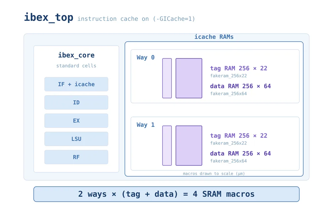
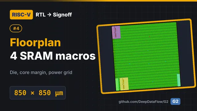
ibex_top with the instruction cache on: 2 ways × (tag + data) = 4 SRAM macros.The RTL is rtl v01 in DDM. The file list's first line, -GICache=1, sets the configuration; the vendor RTL itself is untouched. A small sky130 technology layer does the rest: Ibex asks for a generic single-port RAM, and the sky130 version maps each RAM shape onto a real macro. Clock gating uses a real integrated clock-gating cell from the library instead of a latch that synthesis can't map. All sky130-specific files sit in one folder; everything else is byte-identical to upstream.
Version v01 uses a basic script: generic synthesis, then mapping to the library for area, with no timing information at all. It runs in about 20 seconds: nothing unmapped, about 2,400 registers, four macros. The netlist is checked into DDM as syn v01, so any later step can pull it by version.
Before timing anything, G2's netins tool looks inside the netlist, and reports 1,800 macros. The classifier didn't recognize sky130 cell names, so flip-flops, a few four-input gates, the memories and the clock gate all landed in "macro". You don't need a new G2 release for this. The rules live in a plain text file, mapping.cfg: a pattern, a colon, a category, and the first match wins.
__a4 : Compound
__o4 : Compound
__df : Seq-FF
__sdlclkp : ICG
^fakeram : Memory
Re-run, and the netlist reads as expected: 2,395 flip-flops, four memories, one clock gate. netins also writes a starting SDC from the ports it found: a clock and a default delay on every port. It's a skeleton, not real constraints.
#2Timing-driven synthesis, and choosing with data
 3:57
Watch on YouTube ↗Watch on Bilibili ↗
The skeleton becomes real constraints. The clock is 40 ns at the slow corner. Inputs and outputs get a quarter of the period as external budget, a driving cell and a load make the boundary realistic, test mode is off, and static configuration pins and resets are not timed. The constraints go into DDM as sdc_syn v01; sdc_signoff_func v01 carries the same constraints for now, and gets a version 2 after layout.
Now the catch: Yosys can't optimize to an SDC. Recent versions can parse one, but only to keep the referenced objects. What Yosys has is ABC's delay target, -D, and a constraint file with just a driving cell and a load. And here is the trap: we tried -D alone and the netlist came out byte-identical. ABC only buffers and resizes gates when you also give it -constr.
So the advanced script reads its numbers straight from the SDC: the period, minus the IO budget, minus the uncertainty, is 29 ns for ABC. The driver and the load come from the same file, so there is one source of truth. It also turns on Booth multipliers. The log confirms that ABC got 29,000 ps and the buf_2 driver.
Then OpenSTA judges both netlists, with the same scenario and the same SDC; only the netlist differs.
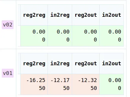
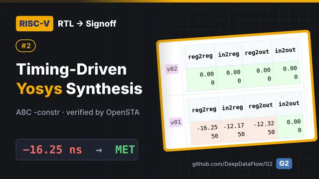
v01 fails every group except input-to-output; timing-driven v02 meets all of them.| v01 basic | v02 timing-driven | |
|---|---|---|
| reg2reg | −16.25 ns | met (+6.65) |
| in2reg | −12.17 ns | met (+13.13) |
| reg2out | −12.32 ns | met (+6.67) |
| Buffers | 0 | 1,494 |
| Standard cells | 16,634 | 17,432 (+4.8%) |
Why does basic fail? Its worst path has one flip-flop driving 259 pins through a minimum-size output: almost 12 ns on a single stage. That is what buffering fixes. Five percent more cells for 23 ns of slack: v02 goes to OpenROAD. These are pre-layout numbers with an ideal clock and no wires, and v02 still has slew violations, which place and route repairs.
Part 2: OpenROAD, one stage per episode
#3Bring the netlist into OpenROAD
 3:55
Watch on YouTube ↗Watch on Bilibili ↗
Place and route needs its own constraints. For a first pass, sdc_apr_func v01 is the synthesis constraints: 40 ns, ideal clock with uncertainty. Later stages switch to the real clock tree. Checking out OpenROAD in G2 gives eight stages, init to finish, and each stage's DDM view lists its inputs.
The init script reads the technology and cell LEFs including the two SRAMs, loads the timing libraries per corner from the MMMC file, reads and links the netlist, and reads the SDC. One change: our netlist is hierarchical, and OpenROAD's hierarchical link mode is still marked as in development, so we link flat.
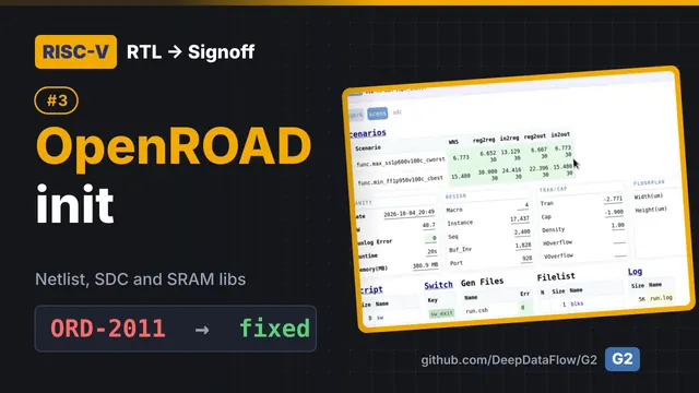
link_design $blkname ;# was: link_design -hier $blknameThe run takes 20 seconds with no errors, but read the warnings: ORD-2011, the two SRAMs have a LEF but no liberty. OpenROAD can place them but can't time them. This release's generator only lists the standard-cell library (fixed in the next version), so we add the memory libraries by hand, slow and fast corner, and don't press Gen again, which would rewrite the file. Every later stage reads it, so one fix covers the flow.
After the fix, worst slack per group at the slow corner matches OpenSTA from episode 2 exactly, reg2reg +6.652 ns: same netlist, same SDC, same libraries. Four macros, 17,400 instances, and the 1,800 buffers and inverters synthesis added. Transition and capacitance still show violations, which placement repairs.
#4Floorplan: die, SRAM macros, power grid
 2:23
Watch on YouTube ↗Watch on Bilibili ↗
The floorplan script makes the die and core, lays down routing tracks, removes the buffers synthesis added (OpenROAD will rebuffer with real placement), places the four SRAMs with a 20 µm halo, inserts tap cells and builds the power grid.
The die and core were the same size, 850 µm with no margin. That would put the SRAMs flush on the die edge, where the IO pins go: pins on top of macros mean shorts at routing, and the power ring would stick out of the die. We leave 10 µm, so the core is 830 µm.
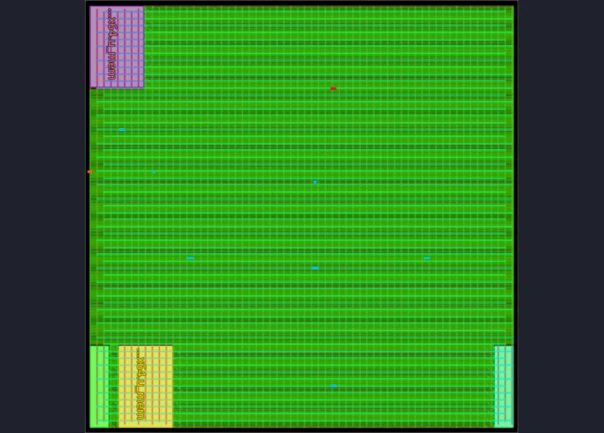
Timing goes red on purpose: reg2reg is −14.7 ns after removing 1,494 synthesis buffers, so long wires drive big loads with tiny cells. The stage added 8,568 tap cells; buffers and inverters dropped from 1,800 to 334; utilization is 31% of the 850 µm die.
#5Placement and design repair
 2:33
Watch on YouTube ↗Watch on Bilibili ↗
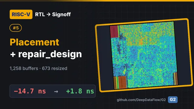
Placement runs a rough global placement that ignores the pins, places the pins next to the logic they connect to, and places again with routing congestion in mind. Then it estimates wires and runs repair_design, which fixes every slew, capacitance and fanout violation by buffering and resizing, and finally legalizes every cell onto a row. It takes about a minute.
repair_design found 710 slew and 235 capacitance violations, inserted 1,258 buffers and resized 673 cells. Timing is back with real placement wires: reg2reg is +1.820 ns, and reg2out misses by 0.63 ns, which post-CTS repairs. No transition or capacitance violations are left, and utilization is 34%.
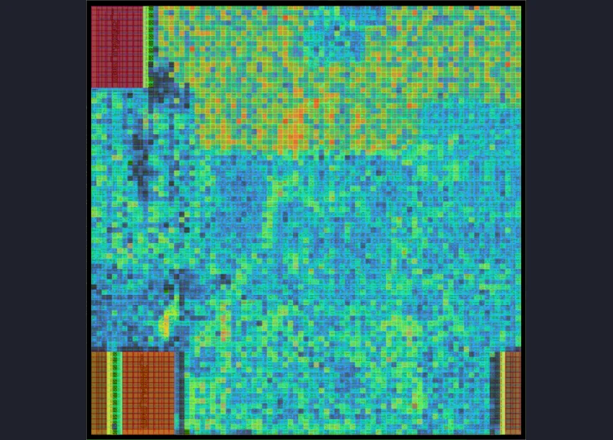
The congestion estimate is hottest over the register file and in the narrow channel beside the left SRAMs. That channel comes back at routing.
#6Clock tree synthesis: zero errors, no tree
 2:34
Watch on YouTube ↗Watch on Bilibili ↗
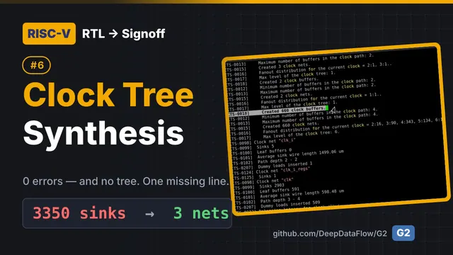
CTS clones clock inverters next to their loads, builds the tree from one buffer type, clkbuf_4, fixes the long wire from the clock pin to the root, and legalizes the new buffers. The first run reports no errors. But the log says clock wires have zero resistance and capacitance, and then CTS thinks the clock has 3,350 macro sinks and skips hundreds of cloned nets. No tree gets built behind the clock gate.
Placement set the wire RC, but that setting isn't saved in the database, and the CTS script never sets it again. Three lines, the same ones placement uses, fix it:
source $fvar(layer_rc)
set_wire_rc -signal -layer $wire_rc_layer
set_wire_rc -clock -layer $wire_rc_layer_clk
Now CTS finds three clock nets: the clock pin feeding the four SRAMs and the clock gate, one flip-flop that isn't gated, and the gated clock behind the core clock gate, which drives almost every register, with 660 buffers. Before the fix that domain had no tree at all, 2,400 flip-flops on one unbuffered net, and the stage still reported zero errors. Read the log, not just the error count.
#7Post-CTS timing repair
 2:18
Watch on YouTube ↗Watch on Bilibili ↗
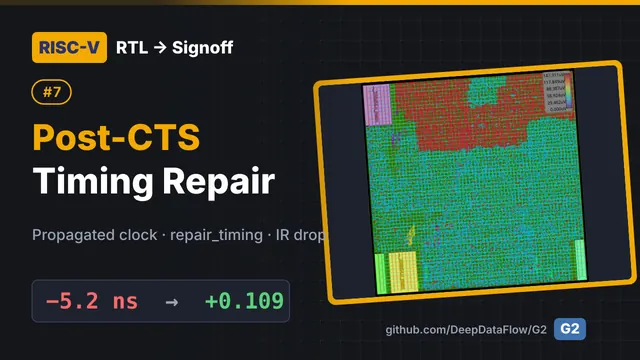
After CTS, timing gets real. The clock switches from ideal to propagated, so every flip-flop sees its actual arrival through the tree. Then repair_timing fixes setup and hold by resizing and buffering, and a static IR-drop check runs on the power grid.
With the real clock, 17 endpoints miss setup: the clock tree adds about 4 ns of delay, which eats into the output budget. repair_timing fixes all of them with eight buffers, from −5.2 ns to +0.109 ns, and hold is met. One net is 160 ps over the slew limit; in a real tapeout we would run repair_design again after CTS. The worst static IR drop is 147 µV, about 0.01% of 1.6 V: the grid is comfortably strong for this design.
#8Global and detailed routing
 2:01
Watch on YouTube ↗Watch on Bilibili ↗
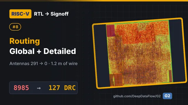
Routing marks constant tie nets as special so the router skips them, finds legal access to every cell pin, plans each net through a coarse grid with up to a hundred extra passes to clear congestion, repairs antennas, and then draws the real metal in ten passes of detailed routing. It runs in the background for about 16 minutes (the runtime card says an hour and a half: that is eight threads added up).
Global route ends with zero overflow, antenna repair takes 291 violations to zero, and detailed route goes from 8,985 violations to 127.
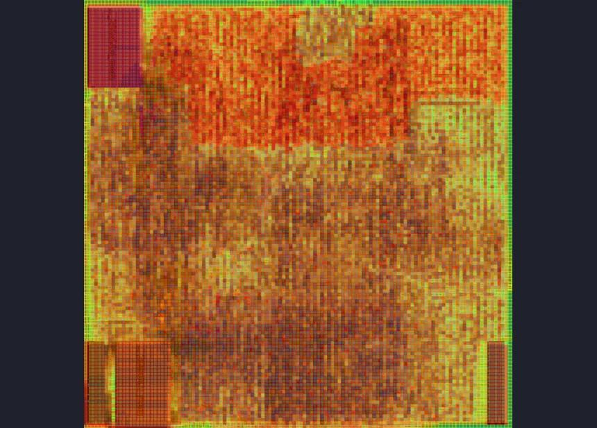
Skip the timing table at this stage: route's report goes back to an ideal clock, so it isn't the real number. Signoff will be.
#9Post-route cleanup and DRC
 1:51
Watch on YouTube ↗Watch on Bilibili ↗
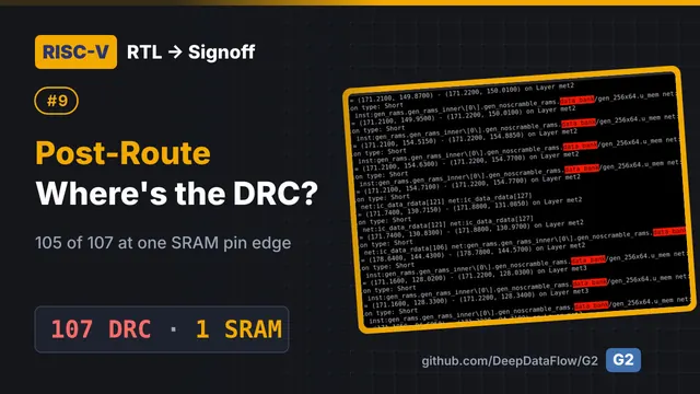
Post-route repairs antennas, recomputes pin access, runs five more detailed-route passes and an antenna loop, and ends with an independent DRC check. It takes about six minutes and leaves 107 violations, 62 of them shorts. The router's own counts go up and down and include duplicates; the DRC card comes from the independent check.
Almost all of them, 105 of 107, are at one SRAM, a data bank of the instruction cache, and the nets right next to it on metal 2 and 3. That SRAM has all 140 signal pins on one metal-3 edge, and the standard cells are packed right up to that edge, so the router has no room to reach the pins. More router passes won't fix that; the floorplan will.
#10Finish: the full chip, and what's left
 2:48
Watch on YouTube ↗Watch on Bilibili ↗
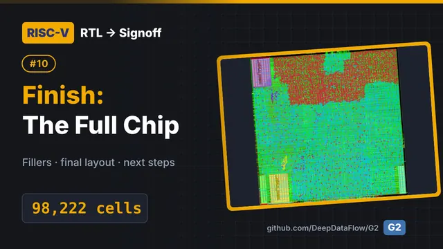
Finish fills the empty row space with filler cells, checks placement and DRC once more, runs IR analysis and writes the DEF, netlist and database. The extraction lines are commented out, so there is no SPEF from here; OpenRCX makes it. The result is 98,222 instances, 70,818 of them fillers, the same 107 DRC as post-route (finish doesn't reroute), and a worst IR drop of about 0.11 mV.
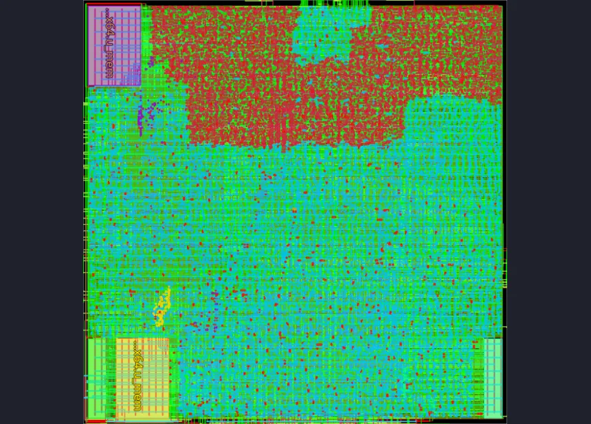
Every stage is on one G2 page, init to finish, each with its log, reports, cards and pictures, and every stage is checked into DDM. If you change one script, you re-run from that stage and compare against this run.
Part 3: Signoff
#11Parasitic extraction with OpenRCX
 2:16
Watch on YouTube ↗Watch on Bilibili ↗
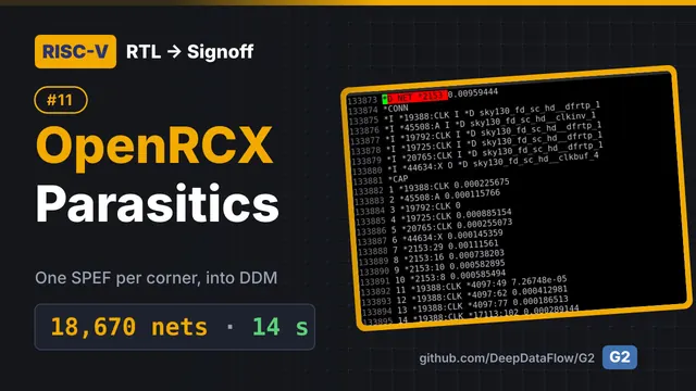
Signoff timing needs the real wires: the resistance and capacitance of every routed net. In G2's flow page, OpenRCX sits next to OpenROAD. Its script reads the finished database (apr_finish v02), and for every corner the project asks for, four from cold to hot, it extracts and writes one SPEF file using that corner's rules file from the PDK spec.
The run takes 14 seconds with no errors: 18,670 nets, 111,215 resistors and 206,593 coupling capacitors. The four SPEF files are the same size, and that's honest: sky130's open rules file has one RC model, so every corner gets the same numbers. A production PDK ships a rules file per corner, and the flow already makes one SPEF per corner, so that's all you'd change. The SPEFs are checked into the same DDM version as the layout, so apr_finish v02 now carries its netlist, DEF and parasitics.
#12Post-route signoff with OpenSTA
 5:14
Watch on YouTube ↗Watch on Bilibili ↗
In episode 2 we judged the netlists with OpenSTA using an ideal clock and no wires. Now the same OpenSTA gets the real layout. The signoff SDC gets a version 2 with three changes: propagated clocks, so OpenSTA follows the real clock tree; smaller uncertainty, from 1 ns to 0.5 for setup and from 0.2 to 0.1 for hold, since skew is now measured; and no clock transition, since real slews come from the tree.
OpenSTA is pointed at apr_finish v02 and its SPEF. One more fix before running: the stock script only checks setup, so the hold card would always read zero, pass or fail. We make it follow the scenario: setup in the max corner, hold in the min corner. Then Merge collects both corners.
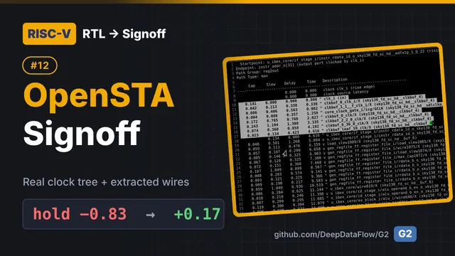
Setup: reg2reg, in2reg and in2out all pass. reg2out misses by 1.74 ns on eight address bits. Follow the clock: it enters at the port, goes through two buffers, the clock gate and four more levels of the tree, and reaches the flip-flop 4.6 ns late at the slow corner. But the output budget still says 10 ns, measured from an ideal clock at the port, so those 4.6 ns come straight out of the budget. That's a conversation with whoever owns the SoC: an output delay that knows about clock latency, or a faster address path. (The 915 "SPEF errors" are nets with no load, and the five missing library cells are fillers and tap cells with no timing.)
Hold passes everywhere at the fast corner, with 0.17 ns to spare on the tightest pair. In episode 10, hold missed by 0.83 ns after routing, but that number came from estimated wires. With extracted wires, hold passes. That's why you sign off on extraction, not estimates. One slew violation is left: 2.2 ns against a 1.5 ns limit.
What we built, and what's left
RTL to signoff with open-source tools, all in G2. DDM holds the whole chip: RTL, constraints, two synthesis versions, every place-and-route stage, the parasitics and two signoff SDCs. Every step pulled its input from there.
What's left, and where to start. Each one is a change to one script or one SDC and a re-run from that step:
- The output budget, −1.74 ns. A constraint to agree with the SoC: an output delay that accounts for clock latency, or a faster address path.
- One slew violation. Run
repair_designagain after CTS. - 107 DRC at one SRAM's pin edge. Give the macros a wider halo in the floorplan, or place them by hand.
- Route-stage timing tables use an ideal clock. Set the propagated clock after reading the SDC.
- One RC model for all corners. A production PDK fixes that.
Watch and keep going
- Videos: the YouTube playlist (English) and the Bilibili collection (Chinese).
- New to G2? Start with G2 Getting Started.
- Next: this core becomes a hard macro inside a real chip in RISC-V SoC: Block to Chip.
- The project: G2_demo_sky130. G2 itself is free as the Community Edition.
- Questions about G2 or running your own flows: support@deepdataflow.com. For licensing and partnerships: sales@deepdataflow.com.