
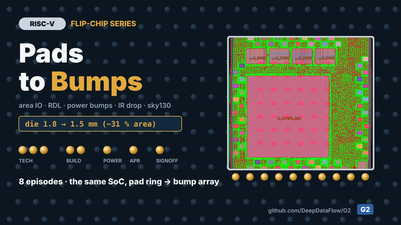
In RISC-V SoC: Block to Chip we built a real chip around a RISC-V core: 58 pads in a ring around the lowRISC Ibex demo system, with the series-1 core as a hard macro. That chip is wirebond: it meets its package through pads on its edge. This series changes how the same chip meets the board, from pads on its edge to bumps on its face.
We remove the pad ring, move the IO cells into the chip under their bumps (area IO), and bring power in through bumps across the core. Then we compare the flip-chip with the wirebond chip on area, the power grid, IR drop, IO timing and core timing. One of those numbers turns out to be less solid than it looks.
This article is the written companion to the 8 videos. Every file is in the G2_demo_sky130 project.
| Starting point | The wirebond chip from RISC-V SoC: Block to Chip: 1.8 mm die, 58 pads, sky130 |
| Change | No pad ring: 58 area-IO cells under their bumps, 7 × 7 power bumps over the core |
| Tools | OpenROAD, OpenRCX and OpenSTA in G2, plus a stand-in redistribution layer |
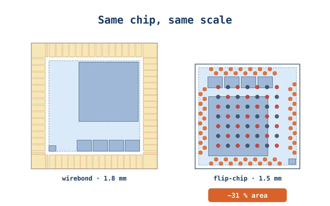
| Area | 1.8 → 1.5 mm per side: −31 % |
| Timing | Hold met; setup −1.61 ns at the core boundary (wirebond: −1.45 ns), the same core budget |
Part 1: Why, and what we need
#1Why flip-chip?
 1:39
Watch on YouTube ↗Watch on Bilibili ↗
The series-2 chip is 1.8 mm square, with 58 pads around a 1.3 mm core. The pad ring is about half the die. The pads, not the logic, set the size: the chip is pad-limited. And every bit of core current comes in through two supply pads, then around the ring.
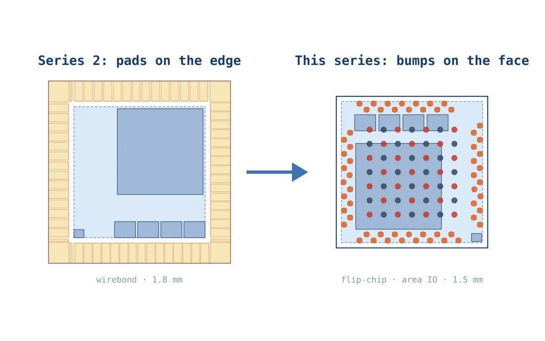
A wirebond chip talks to its package through wires on its edge. A flip-chip is turned face-down onto solder bumps, and a redistribution layer (RDL) connects the bumps to the circuits. There are two ways to do it. You can put bumps on top of the old pad ring, which keeps the ring and the area. Or you move the IO cells into the chip, under their bumps. That is area IO, and that is what we build.
#2A layer above metal 5
 1:13
Watch on YouTube ↗Watch on Bilibili ↗
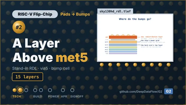
Where would the bumps go? Metal 5 carries the chip's power grid. Metal 4 belongs to the hard core: in series 2 we kept the core off metal 5 so the chip could own the top. So bumps need a layer of their own, above metal 5.
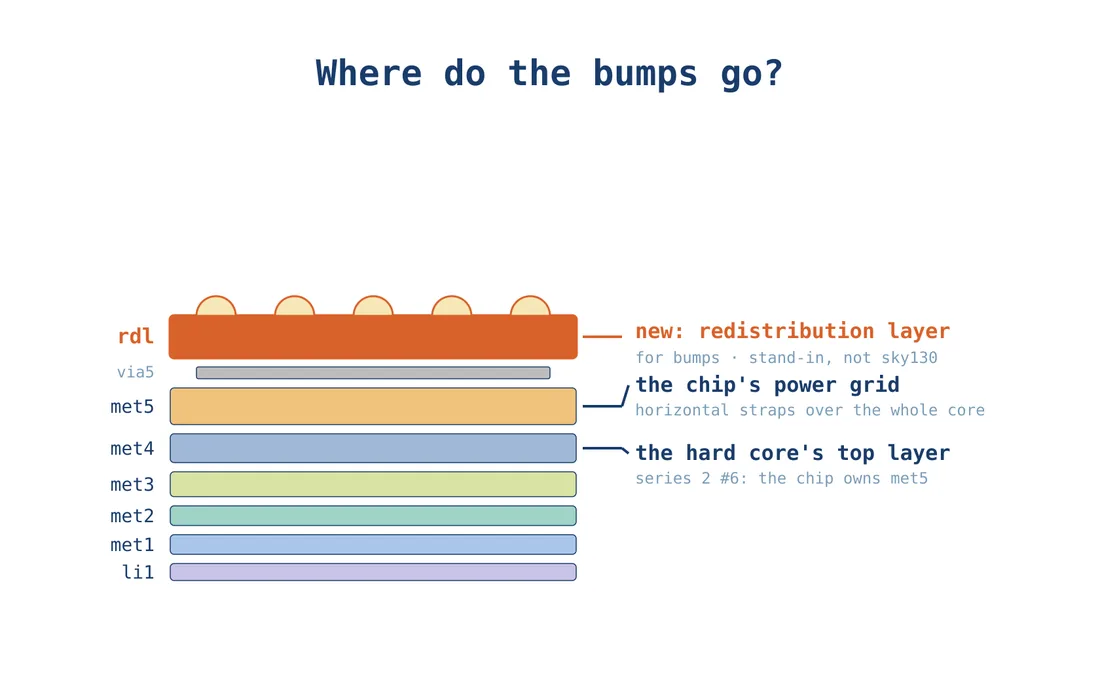
A small script, gen_rdl_tech.py, adds it to a copy of the sky130 technology LEF: a via5 up from metal 5, a thick 10 µm layer called rdl, and a via cell M5RDL between them. The stock sky130 file stays untouched. The bump is a 60 µm octagon on rdl with one pin. The new layers also need resistance values in the RC file: the IR analysis reads resistance from there, not from the LEF, and fails without it. OpenROAD reads the result as 15 layers.
#3Area-IO cells
 1:03
Watch on YouTube ↗Watch on Bilibili ↗
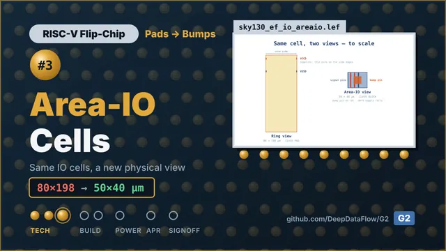
The IO cell from series 2 is 80 × 198 µm, and its supplies are thin pins on its side edges. It only works next to other IO cells, in a ring.
So we make a second physical view of the same cell. It keeps the same name and the same signal pins, so the netlist and the timing libraries don't change. But it is a small block that can sit anywhere: 50 × 40 µm, its bump pin on rdl, and its core supply as metal-4 rails the chip's power grid can reach like any macro's.
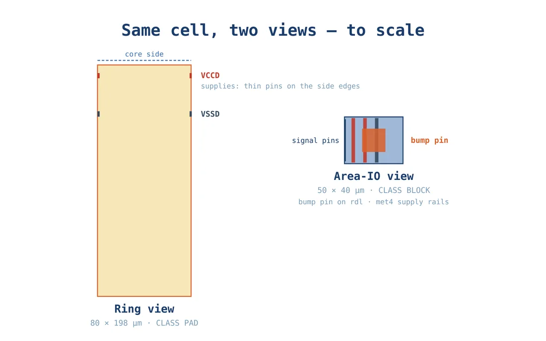
What it doesn't model: the 3.3 V IO supply and the analog side of the pad. Real area-IO libraries have those; ours is a stand-in. A second variant with the bump pin on a metal-2 stub is generated too, for extraction at signoff.
Part 2: The flip-chip floorplan
#4A build without a pad ring
 1:04
Watch on YouTube ↗Watch on Bilibili ↗
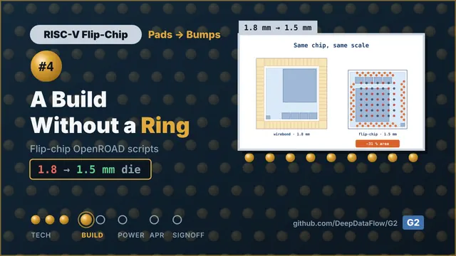
The flip-chip is a new build, v02, next to the wirebond chip, with the same netlist and the same constraints. The design variables change: a 1.5 mm die instead of 1.8, the stand-in technology, the bump, and the area-IO cells instead of the ring cells. Every stage now reads these variables, so every stage sees the new layers.
The floorplan gets two hooks: area IO before macro placement, and bumps after the power grid. The pad ring script is gone, and the core ring no longer looks for pads. Init takes a few seconds, and the log shows 15 layers and the new IO views.
#5IO under bumps
 1:33
Watch on YouTube ↗Watch on Bilibili ↗
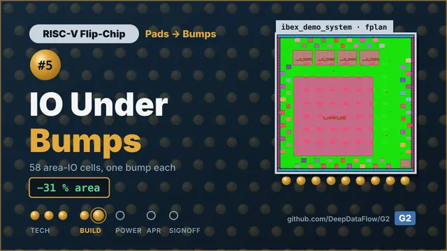
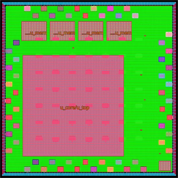
Each IO cell goes into the chip near the edge, in the same order as the old ring, in two staggered rows per side so the bumps fit. Then a bump goes right on top of each IO cell's bump pin. They overlap, so they are connected: no routing is needed for the signals. Bumps are 140 µm apart in a row and at least 92 µm between rows.
The floorplan takes about two minutes. The log shows 58 IO cells placed and 58 IO bumps, and the macro placer finds all 58 IO cells as fixed macros and works around them. The chip has 64 macros, 58 of them IO cells, and a die 1,500 µm wide.
Part 3: Power and IR drop
#6Power bumps and IR drop
 2:05
Watch on YouTube ↗Watch on Bilibili ↗
The power bumps form a 7 × 7 grid over the core, alternating power and ground. Under each one, an array of vias goes down to the metal-5 straps of its own net: 25 power bumps, 24 ground bumps and about 450 vias.
Power and ground are now real chip ports, so the power grid check can run for both, and both are fully connected. The wirebond chip couldn't even be checked this way, because it had no supply ports.
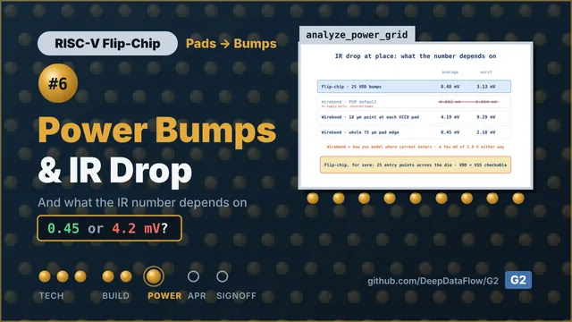
At placement, IR drop analysed from the 25 power bumps is about half a millivolt on average (0.475 mV) and 3.13 mV at the worst point. And the wirebond chip? Its log says 64 µV. The line above explains it: with no supply ports, the tool invented a bump pattern. That number was never real.
So we tell the tool where power really enters the wirebond chip: the two core supply pads. One line per pad gives a position on the core ring, a size and the voltage. We model the same two spots twice:
| Wirebond power entry | Average | Worst |
|---|---|---|
| 10 µm point at each supply pad | 4.19 mV | 9.29 mV |
| The pad's whole 75 µm edge | 0.45 mV | 2.18 mV |
| Flip-chip, 25 power bumps | 0.475 mV | 3.13 mV |
With a 10 µm point, flip-chip looks nine times better. With the whole pad edge, the win is gone.
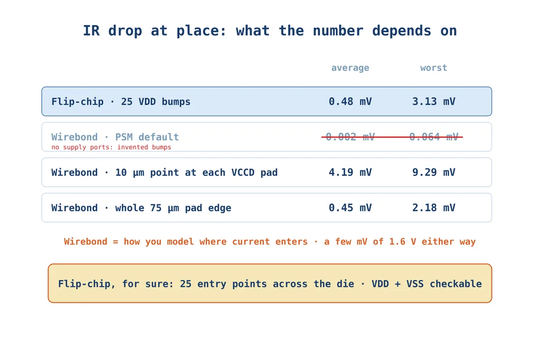
So the wirebond number mostly tells you how you modelled the entry. The real path, through the pad, the ring and the bond wire, isn't in either model. At this chip's power it is a few millivolts out of 1.6 V either way. What flip-chip does give, for sure: power enters at 25 points across the die, which keeps working as power grows, and both power and ground can be checked.
Part 4: Place, route and sign off
#7Place, CTS and route
 1:21
Watch on YouTube ↗Watch on Bilibili ↗
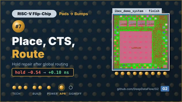
Clock trees and the first hold repair run as in series 2, each stage in under a minute. In practice that wasn't enough: after routing, the real wires cost the debug module about a third of a nanosecond of hold (−0.330 ns on 39 endpoints).
So the route stage gets a hook. Right after global routing, timing is estimated on the routed wires and hold is repaired, before detailed routing. It repairs hold only: a setup repair at this point chased a bad estimate on the output pads and broke detailed routing in practice.
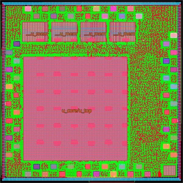
Routing runs for about 13 minutes. The log shows 97 hold endpoints and 31 buffers, and the worst hold goes from −0.539 ns to +0.101 ns. Post-route takes about half an hour and finish three minutes, leaving 8 DRC violations: a demo, not a tape-out. The red output-pad numbers at finish are the same as the wirebond chip's at this stage; signoff checks those paths properly.
#8Signoff and the verdict
 2:17
Watch on YouTube ↗Watch on Bilibili ↗
Signoff starts with extraction, and OpenRCX crashed on our stand-in layer. Worse, the stage still showed zero errors; that is in G2's bug list. The signals never touch the RDL layer in this design, so we extract the die on its own: the bumps and RDL shapes are removed in memory, and the die is extracted with the stock sky130 files. The bumps belong to the package model. Extraction then takes under a minute for four corners.
OpenSTA uses the same script as the wirebond chip, with a slow and a fast corner of about 15 seconds each. Hold is met. Setup misses by 1.61 ns on 226 endpoints, into the debug module's memory: the same core-boundary paths as series 2.
The same IO-path script on both chips prints each port's slack and the part of the path inside the core. Inputs are about 2 ns better on the flip-chip. Outputs are 2 to 2.5 ns worse, and all of it is inside the core, before the pad cell: clock and logic, not the pad. We haven't isolated why. Every IO path still has more than 10 ns of slack.
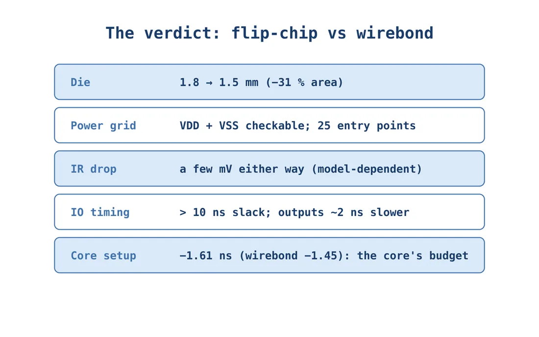
The verdict, and what's left
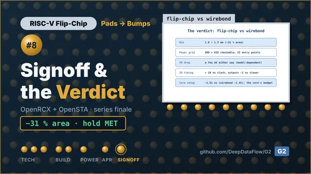
- Area: 31 % less, 1.8 mm to 1.5 mm per side.
- Power grid: power and ground both checkable, with power entering at 25 points across the die.
- IR drop: a few millivolts either way at this power, and the wirebond number depends on how you model it.
- IO timing: every IO path keeps more than 10 ns of slack; outputs are about 2 ns slower, inside the core.
- Core timing: the same budget as before.
What this series did not do: the views are stand-ins, with no DRC, LVS or GDS; the 3.3 V IO supply is not modelled; bump and RDL parasitics are not extracted; the core's setup leftover remains; and 8 DRC violations are left.
Watch and try it
- Videos: the YouTube playlist (English) and the Bilibili collection (Chinese).
- The wirebond chip this series starts from: RISC-V SoC: Block to Chip.
- The project: G2_demo_sky130. G2 itself is free as the Community Edition.
- Questions about G2 or running your own flows: support@deepdataflow.com. For licensing and partnerships: sales@deepdataflow.com.