
Open-source chip tools are usually shown on small designs: a GCD block, a UART, a small RISC-V core. Those demos prove the tools work. They don't show what it takes to run a project at the scale of a real system-on-chip: dozens of blocks, runs that take a day, failed attempts, design data moving between tools and people, and decisions that someone has to be able to explain a week later.
That second part is what G2, our flow manager, is for. To test it on something real, we took a real SoC.
OpenTitan Earlgrey is an open, security-grade RISC-V SoC: about 1.13 million standard cells on SkyWater 130 nm, 23 memories, 70 signal pads, crypto engines, a CPU core and a big-number accelerator. We took it from RTL to a routed, extracted chip with signoff-style static timing, using only open-source EDA tools (Yosys, OpenROAD, OpenRCX, OpenSTA). Every run, input and decision went through G2, and Claude Code, Anthropic's AI coding agent, did much of the hands-on work inside G2's rules.
This first post is the whole arc in one place. The rest of the series goes into each part.
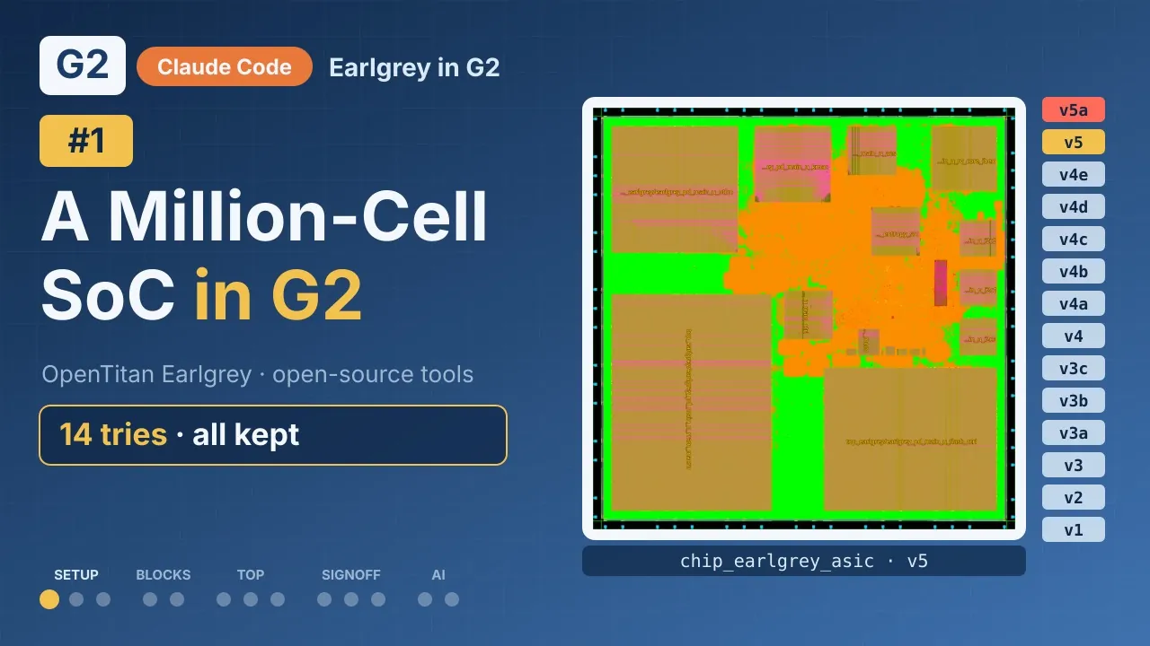 2:27
Watch on YouTube ↗Watch on Bilibili ↗
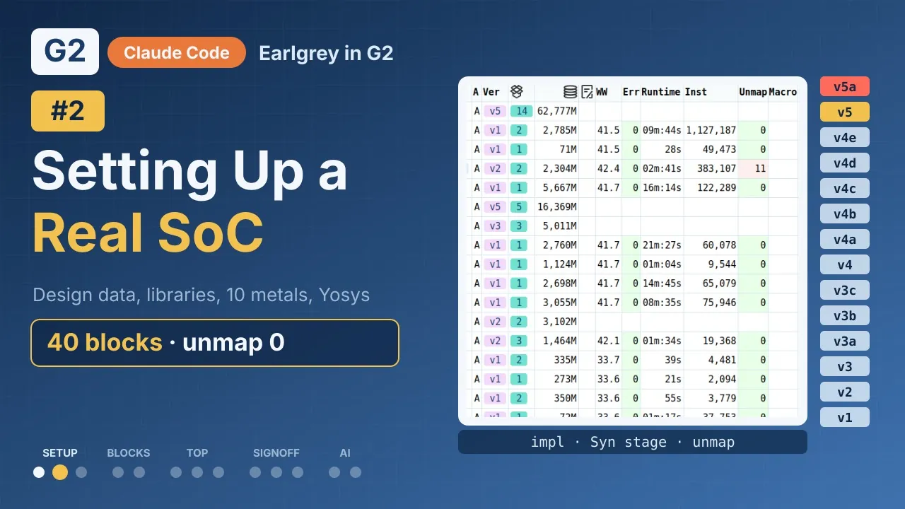 3:22
Watch on YouTube ↗Watch on Bilibili ↗
Where it ended up
The arc in five steps
- Flat hits a wall. All 40 blocks synthesized cleanly with Yosys and yosys-slang. The flat chip then placed in 24.7 hours, 22.5 of them in a single-threaded timing repair, and came out congested everywhere with −164 ns of reg2reg setup slack. It wasn't going to route.
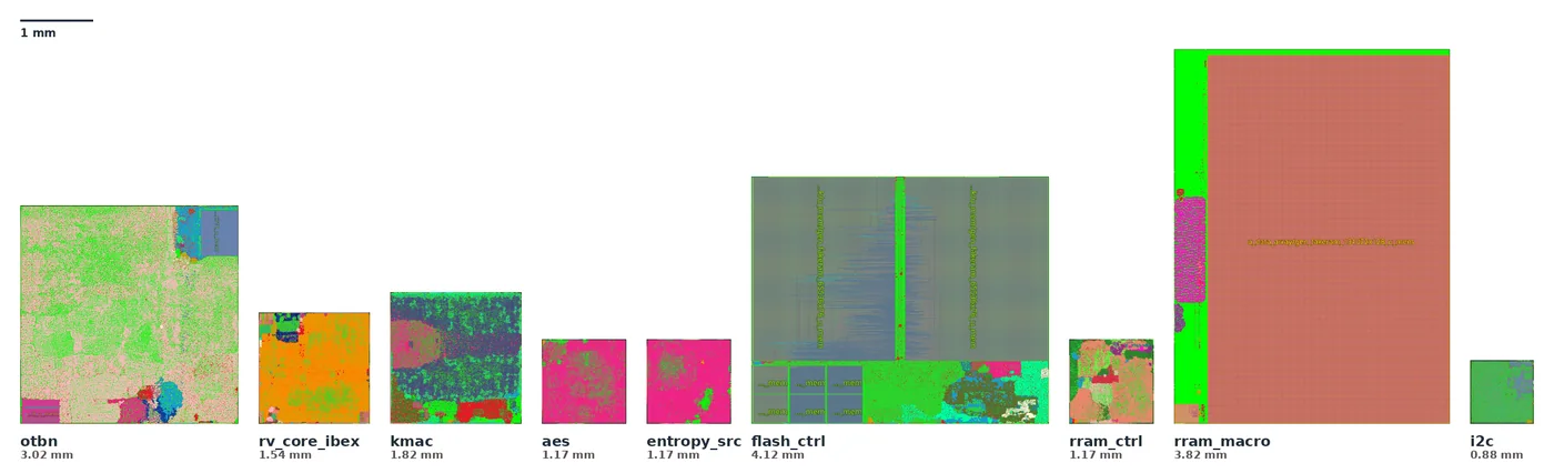
- Hierarchy, the way a chip team would do it. We hardened nine blocks bottom-up: otbn, the Ibex core, kmac, aes, entropy_src, flash and RRAM controllers, the RRAM array and i2c (used three times). Each block went through floorplan, place, CTS and route in G2, was re-timed at the chip clock, and was turned into an IP: an abstract LEF, a two-corner timing model and a black-box stub, registered in G2's library manager. Top-level synthesis and OpenROAD then used them as hard macros. Hierarchical placement took 2.8 hours instead of 24.7.
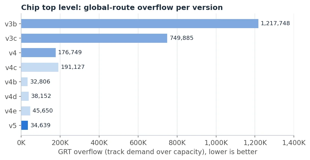
- Making the top level routable, from data. The first top-level global route showed 1.22 million overflowing tracks. Lowering a GRT derate and growing the die helped (176,749 at v4), but not enough. Instead of guessing, we traced where the overflow came from (87% of it over two blocks; the largest single cause was the key manager's logic packed into one channel), built a quick what-if model for block placement, checked the candidates with short global-placement runs, and only then ran the real thing. Version v5 landed at 34,639, close to the level at which the largest block still routed.
- Signoff timing in a separate tool, which found two OpenROAD bugs. As in industry, we did not trust the place-and-route tool's own timing for signoff. We extracted parasitics with OpenRCX and ran standalone OpenSTA on the written netlist and SPEF. That exposed two bugs that only show in a hierarchical flow:
write_spefdropped the module path of objects that CTS creates inside sub-modules, and CTS put its dummy loads in the wrong module, which split 13,566 clock nets in the netlist. We traced both to source, fixed them with regression tests, verified them on the chip, and sent them upstream (OpenROAD issues #11839/#11840, PRs #11841/#11842, still under review). - Checking our own work. After a tool upgrade we ran two checks on the final chip. A power-grid check found the core supply not connected to the pad ring, a real PDN mistake hidden until then. A parasitics probe showed that of 73,824 drivers without SPEF data, only 120 actually drive anything. One finding is bad news, one is good, and both are now in the record.
How G2 kept it manageable
Doing this once by hand would be possible; doing it again, or explaining it afterwards, would not. Five things made the difference:
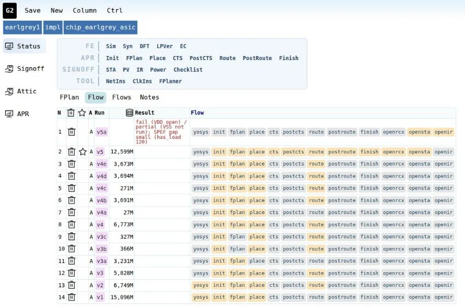
- A new version for every changed run. The chip went through 14 versions (v1 to v5a). Nothing was overwritten, so any number in this series can be traced to the run that produced it.
- Design data and IP as managed objects. RTL, netlists, SDC and each place-and-route stage are versioned and published in G2's design data manager; hardened blocks are entries in its library manager, not files copied between directories.
- A written decision trace. Every non-obvious choice got a line: what was decided, when, and why. A hundred and one of them were logged in seven days.
- Claude Code working inside those rules. In one unattended night it diagnosed and fixed four route failures on the largest block, generated the hard-macro views of seven blocks and logged sixteen decisions with reasons. It also made mistakes. In the SPEF bug it first blamed the wrong tool, and the engineer's question about what the writer got right led to the real cause. We'll come back to how that collaboration works.
- Hard limits. One EDA job at a time, 10 threads, a 22 GB memory cap per job. At this scale memory decides what can run, not CPU.
What this is not
None of that changes the main result: with open tools, an AI agent and a flow manager that keeps track of everything, a million-cell SoC is a project you can actually run, explain and repeat. And it ran on a laptop: the chip's placement and routing ran on one machine with an Intel Core Ultra 7 155H (22 threads) and 30 GB of RAM, with a few small machines on Slurm for the lighter jobs. The hard parts are scale, memory and making several tools agree on one design, and those are the parts the rest of this series is about.